|
<< Click to Display Table of Contents >> Single Line Diagram |
  
|
|
<< Click to Display Table of Contents >> Single Line Diagram |
|
Note: This feature has been introduced in PVsyst V7.3.0 and is still work in progress. It can happen that the PV system is too complex to be converted into the single line diagram. Furthermore there might be special cases where the program does not succeed to create the single line diagram. In this case you will be prompted with an error message saying that the diagram could not be created. It would be of great help if in such cases you could give feedback to support@pvsyst.com, describing the case where the single line diagram was not created successfully.
Currently the single line diagram is only available for grid connected systems, standalone and pumping systems will follow in a future PVsyst version. The single line diagram contains PV module strings, inverters and transformers. It does not include possible storage systems.
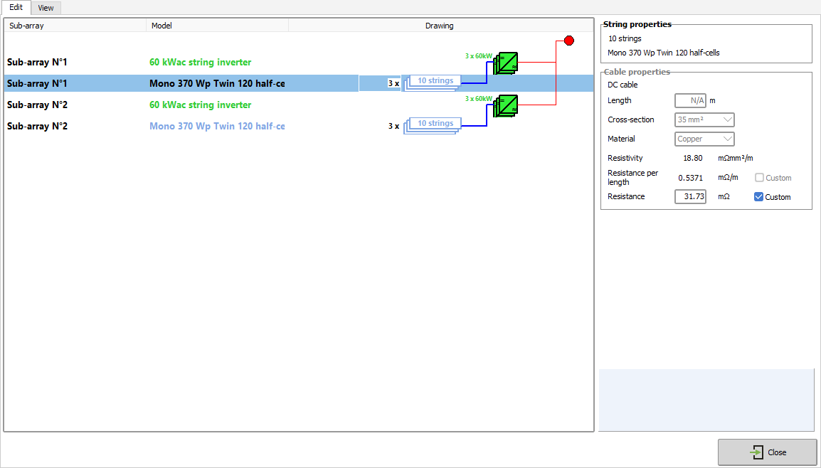
The single line diagram window is accessible from the 'System' dialog as well as from the 'Detailed losses - Ohmic Losses' dialog. Clicking on the button ![]() will open a window with two tabs called 'Edit' and 'View'. The window of the single line diagram can be kept open while editing the 'System' or 'Ohmic losses'. The changes made in these dialogs will be immediately visible in the single line diagram.
will open a window with two tabs called 'Edit' and 'View'. The window of the single line diagram can be kept open while editing the 'System' or 'Ohmic losses'. The changes made in these dialogs will be immediately visible in the single line diagram.
Single line diagram editor
The editor of the single line diagram allows to see the tree structure of the system circuit on the left side. The properties of the selected node are displayed on the right side.The different nodes are the components like strings, inverters, combiner boxes, transformers, and so on. They are connected by cables which are drawn in blue for the DC part of the circuit and in red for the AC part. Each node is a line in the tree view with two column entries on the left. The first column indicates the sub-array from 'System' to which this node belongs. The second column contains information on PV module and inverter types.
Each node has a single set of outgoing cables that link it to its parent node. The cable properties displayed on the right side are always the properties of the outgoing cables of the selected node.
Single line diagram editing tab
Currently the editor allows only a very reduced number of operations on the circuit, mainly consisting in grouping or un-grouping the nodes. In future PVsyst versions this options will increase and eventually it will become possible to edit the components from within this circuit view. So far there is no undo-function in the editor, we therefore recommend to be careful with the ungrouping functions, as they may lead to large trees that are difficult to work with.
The nodes can represent a single object or groups of several objects. The grouping is only possible if the nodes are identical, including all its children. The properties of the different types of nodes are explained below. If the node consists of a group of components, the children nodes are shown only once. To make clear that each of these children exists in each component of the group, the multiplicity is shown left to the child node. In the example above, there are two groups of three inverters each. Each inverter has a group of ten strings connected to it. The transformer nodes are an exception to this, if they represent a group, all children will be represented in the diagram (see also the explanation of transformer nodes in the following).
The top node of the single line diagram is always the injection point. From this top node the circuit branches according to the definitions made for the current variant. The following paragraphs give a short description of the currently possible node types.
![]()
There is only one single injection point in the diagram. It does not have any outgoing cable.

There can be nodes for MV and HV transformers. There can be only one HV transformer node, and consists always of one single element. On the other hand, the re can be several MV transformer nodes, and these nodes can be groups. If a MV transformer node is a group, the children nodes are not meant to be multiplied by the number of transformers. This is an exception from all other nodes that can be groups and have children, like inverters, MPPT inputs and combiner boxes.
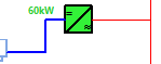
Inverter nodes have DC cables at their input and AC cables going out. Grouping inverter nodes is currently only possible with nodes containing a single inverter. This means that if you would like to join a single inverter or a group of inverters to another group of inverters you need to ungroup them first.
![]()
Currently the combiner boxes are only possible in the DC part of the circuit. If the DC cables in the 'Ohmic losses' dialog have been defined via the 'Detailed computation' tool there can be one or two levels of combiner boxes between the inverters and the strings. In these cases the cable lengths are also defined and will show up in the diagram.

The MPPT inputs of the inverters are represented as separate nodes in the diagram, even if they are physically integrated in the inverters. The MPPT nodes do not have cable definitions, although a blue line is drawn between them and the parent inverter node.
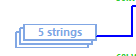
The strings are represented by blue rectangles and represent the end points of the tree structure in the diagram. Therefore they do not have any incoming cables. Grouping and ungrouping of strings on the same inverter or MPPT input is always possible.
Each node, except for the injection point node, has an outgoing cable to the right. In the DC part of the circuit the cables are drawn in blue, while for the AC part they are drawn in red. If the cable properties are defined in the 'Detailed losses' dialog, then the cable is drawn in bold, else it will be a simple line. The cable properties, if defined, are indicated on the right side. There are two ways for displaying the cable properties, either by their resistance, or by their length, cross-section and material. The display will follow the way the cables where defined in the tab 'Ohmic losses' from the window 'Detailed losses'. If the cables have a defined length, it will also be displayed next to the cable itself, as in the example of the combiner box above.
In many cases it is not convenient to display each element of the PV system in a separate node. Therefore, elements with identical properties can be grouped. To check if two nodes are identical and can be grouped, also all children are considered. By default, the single line diagram will try to group as many nodes as possible. You have the possibility to un-group these nodes in the editor, and this will propagate also to the viewer. We recommend to avoid un-grouping groups with many elements, since this will make the single line diagram hard to read.
When the components of the circuit are edited in the 'System' or 'Ohmic loss' dialog, PVsyst will update the single line diagram, while trying to keep the grouping/ungrouping that has already been performed. This is not always easily possible, and for example it might happen that when changing the number of strings in a sub-array a set of strings that had been ungrouped collapses back to a single group. We therefore recommend, if possible, to leave any grouping steps to the end of the system design, when the number of components will not change any more.
To un-group or group nodes, you need to select them first and then do a right-click with the mouse on them. This will open a context menu with the options 'group', 'ungroup' and 'custom group'. The different options will only be active if the selected nodes allow for this functionality. If for example only nodes with single strings are selected, the un-grouping will not be possible. Similarly, if non-identical nodes are selected, the grouping function will not be available.
When selecting 'ungroup', the program will split a node into nodes with single elements. For nodes with many elements this is not very practical. In these cases, the function 'custom group' allows you to reorganize a node or a selection of nodes into a given number of groups. When selecting this function, a small dialog pops up which allows to regroup the elements. You can either provide the number of groups that should be created, or the number of elements that should be in each group. If the total number of elements is not a multiple of these two figures, then two kinds of groups will be created, which will differ only by one in the number of elements.
Example:
In the following example a node with 192 elements, strings in this case, is split into five groups. As can be seen, this results in 3 groups of 38 strings and two groups of 39 strings, making for a total of 192 strings. Note that this grouping result is now set for all four inverters in this example. Ungrouping the inverters would yield 4 inverter nodes, each one with 5 groups of strings identical to the right side of the example.
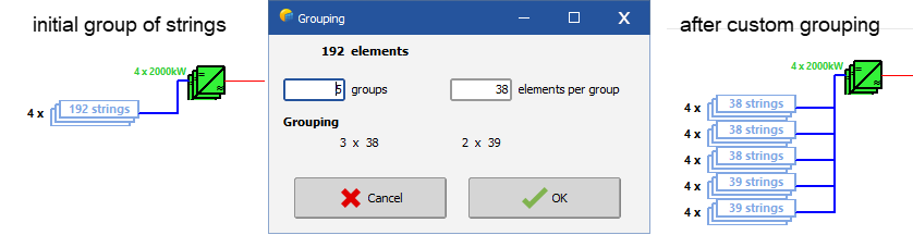
If instead of choosing the number of groups, we would have entered 38 for the number of elements, the grouping would have been done differently. The algorithm builds as many groups of 38 elements as possible, and puts the remaining elements, if any, into one separate group.
Single line diagram viewer
The viewer of the single line diagram shows a drawing of the system circuit. several parameters driving the rendering of the diagram can be customized, and the drawing can be sent to a printer. It is also possible to include this drawing of the single line diagram in the PVsyst report. Clicking and dragging on the drawing will move the paper, while the mouse wheel allows to zoom in or out.
Single line diagram view tab
In this group of controls you can choose to have the diagram in portrait or landscape orientation. The supported paper sizes are A1 - A4 as well as US letter and legal.
A part of this functionality is also replicated in the toolbar on the top of the window. There is a button to toggle the orientation and two shortcuts for A4 and A3 paper format.
The option group allows to toggle the visibility of the labels, and to include or exclude the legend at the bottom of the diagram. There is also a slider to zoom in and out. The zooming function is also accessible via the mouse wheel or the two buttons in the toolbar.
If the option 'Center on injection point' is checked, the injection point will be vertically centered on the diagram, and the child nodes will exit to the top and to the bottom. Each node in the diagram will position its children in a similar way.
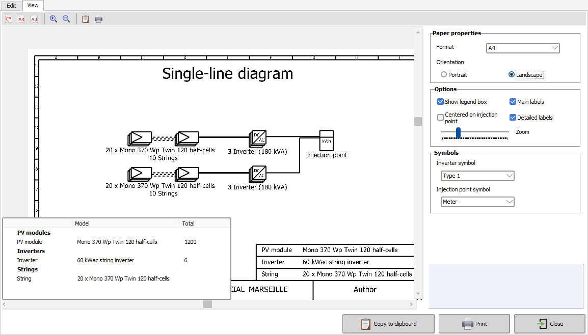
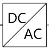
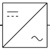
In the 'Symbols' group you can choose how the inverters and the injection point are drawn.
There are three options for the inverters:
and three options for the injection point:
![]()
![]()
The Print buttons open the print preview for the single line diagram. There is one print button at the bottom of the dialog, and one in the toolbar on the top.
In the print preview you can set the client logo via the 'Report options'. For the output you can either send this page directly to a printer, save it as a PDF file or copy the page as a picture to the windows clipboard, so that it can be pasted in another document.
The single line diagram can also be included in the report. In the report preview in 'Report options' -> 'Final report option' you can select the pages that should be included in the report. Here, also the single line diagram can be selected or deselected.